DEMO22
Mobile lab for project 5D Printing
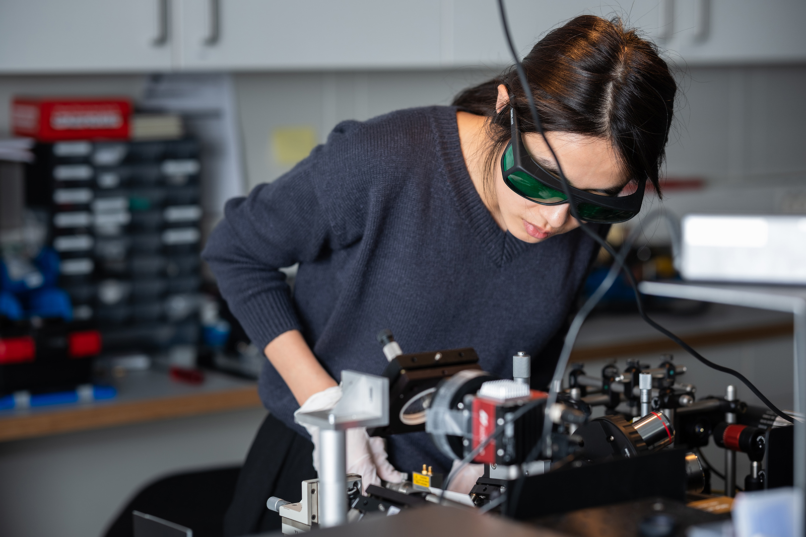
The project addresses central objectives of the InnovationCampus Future Mobility in the area of “Mobility and Additive Manufacturing”. The focus is on large 3D-printed optics for sensors for autonomous driving. These optics must be measured with high precision in order to ensure their imaging quality - currently a technically demanding challenge. The project is pursuing a novel approach to wavefront measurement of these optics that is compact, cost-effective and practical. Close cooperation between physics and engineering sciences as well as with industrial partners such as Nanoscribe and the spin-off Printoptix GmbH will ensure rapid transfer to industrial applications.
A special feature of the project is the clear presentation of the measurement results: The mobile demonstrator is to be used specifically to make complex optical technologies understandable and tangible for schoolgirls, students and interested visitors - for example as part of events, laboratory visits or science festivals.
Aim
The aim of the project is the high-precision measurement of 3D-printed lenses for sensors for autonomous vehicles. The aim is to detect and correct errors in the optical image caused by inaccuracies during 3D printing at an early stage.
Approach
The demonstration project makes complex measurement technology understandable for a wide audience: with the help of a phase camera, the measured wavefronts are clearly visualized so that schoolchildren, students and other visitors can intuitively understand how incorrectly printed lenses lead to image distortions in sensor systems.
Benefits
The measurement technology enables a significant improvement in the imaging quality of 3D-printed optics. This avoids image errors that would later impair the function of sensor systems - for example when detecting pedestrians or other road users.
For production, this means:
- Greater safety thanks to more precise sensor data in autonomous vehicles
- More efficient production thanks to direct quality control of the optics
Key data
Research Field
Period
01.01.2024 until 31.10.2024Project participants
- University of Stuttgart: 4th Physics Institute (PI4, Prof. Harald Giessen)
- Involved companies: Printoptix GmbH, Stuttgart, as well as Nanoscribe GmbH & Co. KG, Karlsruhe
Contact
Thilo Zimmermann
Deputy Managing Director, Head of Research Coordination
- Phone
- +49 711 685 60960
- fk@icm-bw.de